- 您现在的位置:买卖IC网 > Sheet目录3875 > PIC18F44J10T-I/ML (Microchip Technology)IC PIC MCU FLASH 8KX16 44QFN
Micrel, Inc.
KSZ8851SNL/SNLI
August 2009
71
M9999-083109-2.0
Absolute Maximum Ratings
(1)
Supply Voltage (VDD_A3.3, VDD_IO) ......... –0.5V to +4.0V
Input Voltage (All Inputs).............................. –0.5V to +4.0V
Output Voltage (All Outputs) ........................ –0.5V to +4.0V
Lead Temperature (soldering, 20sec.) ....................... 260°C
Storage Temperature (Ts) ......................... –65°C to +150°C
Maximum Junction Temperature (TJ)....................... +125°C
HBM ESD Rating .......................................................... 6KV
Operating Ratings
(2)
Supply Voltage
VDD_A3.3 .......................................... +3.1V to +3.5V
VDD_IO (3.3V) ................................... +3.1V to +3.5V
VDD_IO (2.5V) ............................... +2.35V to +2.65V
VDD_IO (1.8V) ................................... +1.7V to +1.9V
Ambient Operating Temperature (TA)
Commercial (SNL)…………….……………...0°C to +70°C
Industrial (SNLI)……………….…………...-40°C to +85°C
Thermal Resistance
(3)
Junction-to-Ambient (
θ
JA) ...............................34°C/W
Junction-to-Case (
θ
JC) ......................................6°C/W
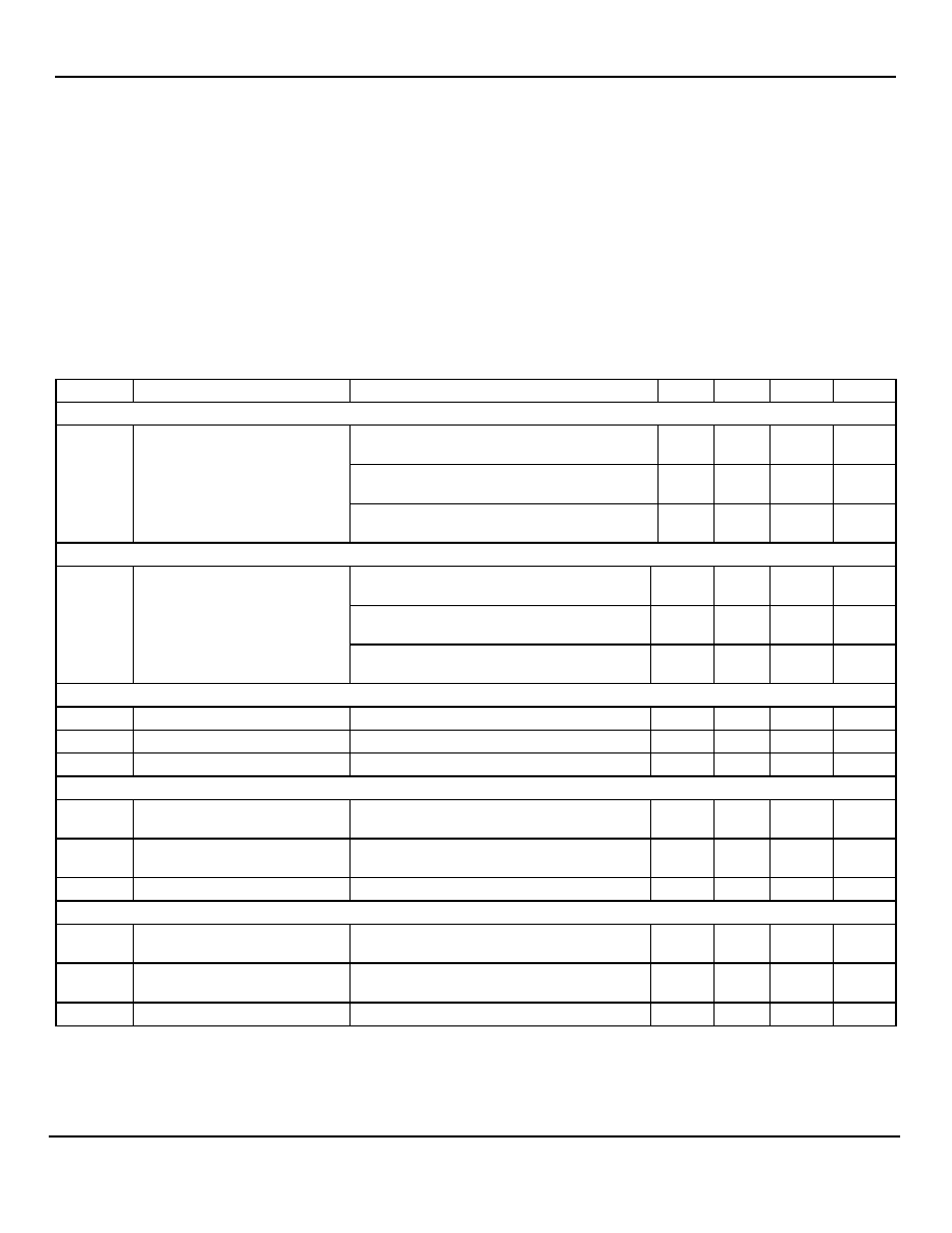
Electrical Characteristics
(4, 5)
Symbol
Parameter
Condition
Min
Typ
Max
Units
Supply Current for 100BASE-TX Operation (Single Port@100% Utilization)
VDD_A3.3, VDD_IO = 3.3V; Chip only (no
transformer)
85
mA
VDD_A3.3=3.3V, VDD_IO = 2.5V; Chip only
(no transformer)
85
mA
Idd1
100BASE-TX
(analog core + PLL + digital
core + transceiver + digital I/O)
VDD_A3.3=3.3V, VDD_IO = 1.8V; Chip only
(no transformer)
85
mA
Supply Current for 10BASE-T Operation ( Single Port@100% Utilization)
VDD_A3.3, VDD_IO = 3.3V; Chip only (no
transformer)
75
mA
VDD_A3.3=3.3V, VDD_IO = 2.5V; Chip only
(no transformer)
75
mA
Idd2
10BASE-T
(analog core + PLL + digital
core + transceiver + digital I/O)
VDD_A3.3=3.3V, VDD_IO = 1.8V; Chip only
(no transformer)
75
mA
Power Management Mode
Idd3
Power Saving Mode
(6)
Ethernet cable disconnected & Auto-Neg
70
mA
Idd4
Soft Power Down Mode
Set Bit [1:0] = 10 in PMECR register
2
mA
Idd5
Energy Detect Mode
At low power state
2
mA
TTL Inputs (VDD_IO = 3.3V/2.5V/1.8V)
VIH
Input High Voltage
2.0/2.0
/1.3
V
VIL
Input Low Voltage
0.8/0.6
/0.3
V
IIN
Input Current
VIN = GND ~ VDD_IO
-10
10
A
TTL Outputs (VDD_IO = 3.3V/2.5V/1.8V)
VOH
Output High Voltage
IOH = -8mA
2.4/1.9
/1.5
V
VOL
Output Low Voltage
IOL = 8mA
0.4/0.4
/0.2
V
|IOZ|
Output Tri-state Leakage
10
A
Notes:
1.
Exceeding the absolute maximum rating may damage the device.
2.
The device is not guaranteed to function outside its operating rating. Unused inputs must always be tied to a appropriate logic voltage level (Ground
to VDD_IO).
3.
No (HS) heat spreader in this package. The
θ
JC/θJA is under air velocity 0m/s.
4.
TA = 25°C. Specification for packaged product only.
发布紧急采购,3分钟左右您将得到回复。
相关PDF资料
PIC18LF24J10T-I/ML
IC PIC MCU FLASH 8KX16 28QFN
DSPIC30F6011T-20E/PF
IC DSPIC MCU/DSP 132K 64TQFP
DSPIC30F6010T-20E/PF
IC PSPIC MCU/DSP 144K 80TQFP
DSPIC30F4013T-20I/PT
IC DSPIC MCU/DSP 48K 44TQFP
DSPIC30F4013T-20I/ML
IC DSPIC MCU/DSP 48K 44QFN
DSPIC30F4012T-20I/SO
IC DSPIC MCU/DSP 48K 28SOIC
DSPIC30F4012T-20I/ML
IC DSPIC MCU/DSP 48K 44QFN
PIC24F16KL402-I/SO
IC MCU 16BIT 16KB FLASH 28-SOIC
相关代理商/技术参数
PIC18F44J10T-I/PT
功能描述:8位微控制器 -MCU 16 KB FL 1024 RAM RoHS:否 制造商:Silicon Labs 核心:8051 处理器系列:C8051F39x 数据总线宽度:8 bit 最大时钟频率:50 MHz 程序存储器大小:16 KB 数据 RAM 大小:1 KB 片上 ADC:Yes 工作电源电压:1.8 V to 3.6 V 工作温度范围:- 40 C to + 105 C 封装 / 箱体:QFN-20 安装风格:SMD/SMT
PIC18F44J11-I/ML
功能描述:8位微控制器 -MCU 16KB Flash 4KBRAM 12MIPS nanoWatt RoHS:否 制造商:Silicon Labs 核心:8051 处理器系列:C8051F39x 数据总线宽度:8 bit 最大时钟频率:50 MHz 程序存储器大小:16 KB 数据 RAM 大小:1 KB 片上 ADC:Yes 工作电源电压:1.8 V to 3.6 V 工作温度范围:- 40 C to + 105 C 封装 / 箱体:QFN-20 安装风格:SMD/SMT
PIC18F44J11-I/PT
功能描述:8位微控制器 -MCU 16KB Flash 4KBRAM 12MIPS nanoWatt RoHS:否 制造商:Silicon Labs 核心:8051 处理器系列:C8051F39x 数据总线宽度:8 bit 最大时钟频率:50 MHz 程序存储器大小:16 KB 数据 RAM 大小:1 KB 片上 ADC:Yes 工作电源电压:1.8 V to 3.6 V 工作温度范围:- 40 C to + 105 C 封装 / 箱体:QFN-20 安装风格:SMD/SMT
PIC18F44J11T-I/ML
功能描述:8位微控制器 -MCU 16KB Flash 4KBRAM 12MIPS nanoWatt RoHS:否 制造商:Silicon Labs 核心:8051 处理器系列:C8051F39x 数据总线宽度:8 bit 最大时钟频率:50 MHz 程序存储器大小:16 KB 数据 RAM 大小:1 KB 片上 ADC:Yes 工作电源电压:1.8 V to 3.6 V 工作温度范围:- 40 C to + 105 C 封装 / 箱体:QFN-20 安装风格:SMD/SMT
PIC18F44J11T-I/PT
功能描述:8位微控制器 -MCU 16KB Flash 4KBRAM 12MIPS nanoWatt RoHS:否 制造商:Silicon Labs 核心:8051 处理器系列:C8051F39x 数据总线宽度:8 bit 最大时钟频率:50 MHz 程序存储器大小:16 KB 数据 RAM 大小:1 KB 片上 ADC:Yes 工作电源电压:1.8 V to 3.6 V 工作温度范围:- 40 C to + 105 C 封装 / 箱体:QFN-20 安装风格:SMD/SMT
PIC18F44J50-I/ML
功能描述:8位微控制器 -MCU Full Spd USB 16KB 4KBRAM nanoWatt RoHS:否 制造商:Silicon Labs 核心:8051 处理器系列:C8051F39x 数据总线宽度:8 bit 最大时钟频率:50 MHz 程序存储器大小:16 KB 数据 RAM 大小:1 KB 片上 ADC:Yes 工作电源电压:1.8 V to 3.6 V 工作温度范围:- 40 C to + 105 C 封装 / 箱体:QFN-20 安装风格:SMD/SMT
PIC18F44J50-I/PT
功能描述:8位微控制器 -MCU Full Spd USB 16KB 4KBRAM nanoWatt
RoHS:否 制造商:Silicon Labs 核心:8051 处理器系列:C8051F39x 数据总线宽度:8 bit 最大时钟频率:50 MHz 程序存储器大小:16 KB 数据 RAM 大小:1 KB 片上 ADC:Yes 工作电源电压:1.8 V to 3.6 V 工作温度范围:- 40 C to + 105 C 封装 / 箱体:QFN-20 安装风格:SMD/SMT
PIC18F44J50T-I/ML
功能描述:8位微控制器 -MCU Full Spd USB 16KB 4KBRAM nanoWatt RoHS:否 制造商:Silicon Labs 核心:8051 处理器系列:C8051F39x 数据总线宽度:8 bit 最大时钟频率:50 MHz 程序存储器大小:16 KB 数据 RAM 大小:1 KB 片上 ADC:Yes 工作电源电压:1.8 V to 3.6 V 工作温度范围:- 40 C to + 105 C 封装 / 箱体:QFN-20 安装风格:SMD/SMT